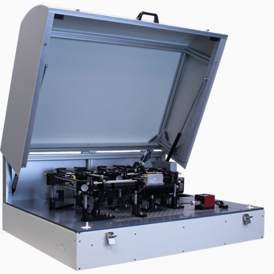
Linseis – Αναλυτής Λέιζερ Λεπτών Υμενίων (Laser Flash Analyzer for Τhin Films TF-LFA)
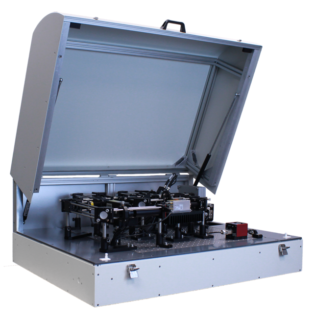
Ο αναλυτής TF-LFA (Thin Film Laser Flash Analyzer) της Linseis, είναι ένα προηγμένο όργανο για τη μέτρηση της θερμικής αγωγιμότητας και διαχυτικότητας σε λεπτά υμένια πάχους 10 nm έως 20 µm. Υποστηρίζει ανάλυση θερμικών ιδιοτήτων κατά τον άξονα και την επιφάνεια (cross-plane/in-plane) με μη καταστροφικές μεθόδους και υψηλή ακρίβεια. Είναι ιδανικό για εφαρμογές σε ημιαγωγούς, LEDs και θερμοηλεκτρικά υλικά, με δυνατότητα λειτουργίας σε ευρύ θερμοκρασιακό εύρος και λεπτομερή χαρτογράφηση θερμικών ιδιοτήτων.
Laser Flash Analyzer for thin films (TF-LFA)
Determining the thermo-physical properties of materials and optimizing heat flows in end products is becoming increasingly important for many industrial applications.
For this reason, the flash method has become the most commonly used technique for measuring the temperature and thermal conductivity of various solids, powders and liquids in recent decades.
In the age of nanotechnology, more and more industries and users now require precise measurement data for very thin layers. The semiconductor industry with typical products such as light-emitting diodes (LEDs), phase-change memories or flat screens has the greatest demand.
Several layers of different materials are often deposited on a substrate in order to create a component with a specific function. Since the physical properties of thin films usually differ from those of a solid material, their characterization is essential for the design and optimization of thermal management.
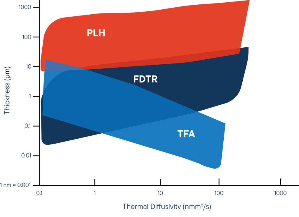
Based on the proven laser flash technology, the Linseis Laserflash for Thin Films (TF-LFA) now offers a whole range of new possibilities for analyzing the material data of thin films with a thickness of 10 nm to 20 µm.
Thermal properties:
✔️Thermal conductivity
✔️Volumetric heat capacity
✔️Thermal diffusivity
✔️Thermal efficiency
✔️Thermal limit conductivity
Thin films:
Thin films are materials with a thickness of nanometers to micrometers that are applied to surfaces.
Their thermophysical properties differ considerably from those of bulk materials and depend on thickness and temperature.
Thin films are generally used in semiconductors, LEDs, fuel cells and optical storage media.
Different types of thin films
- Thin film: layer from a few nm to µm
- Layers are grown on a special substrate
- Typical growth techniques are
⚬ PVD (e.g. sputtering, thermal vaporization)
⚬ CVD (PECVD, LPCVD, ALD)
⚬ Drop casting, Spin coating & Printing
- Many different types of layers, including:
⚬ Semiconductor layers (e.g. thermoelectric, sensors, transistors)
⚬ Metallic layers (used as contacts)
⚬ Thermal barrier coatings
⚬ Optical coatings
Downloads
ΙΔΑΝΙΚΟ ΓΙΑ
The Linseis TF-LFA is ideal for applications requiring detailed thermal property analysis of thin films and layered structures, particularly in:
- Semiconductors: Characterizing thermal properties critical for microelectronics and integrated circuits.
- Thermoelectrics: Evaluating materials for energy conversion efficiency.
- LEDs and Optoelectronics: Measuring heat dissipation in light-emitting devices.
- Nanotechnology: Thermal management of nanostructures and ultrathin materials.
- Coatings and Interfaces: Analyzing thermal resistance in multi-layered and thin-film coatings
These capabilities support research and development in advanced materials and thermal management technologies.
ΧΑΡΑΚΤΗΡΙΣΤΙΚΑ
MODEL |
TF-LFA |
|---|---|
| Sample dimensions: | Any shape between 2mm x 2mm and 25mm x 25mm lateral size |
| Thin film samples: | 10nm up to 20μm* (depends on sample) |
| Temperature range: | RT, RT up to 200/500°C Sample holder for 4“ Wafer (only RT) |
| Measured properties: | Thermal conductivity Thermal diffusivity Thermal interface resistance Volumetric specific heat capacitiy Thermal effusivity |
| Options: | Anisotrophy: Measurement of cross-plane and in-plane thermal properties Sample mapping: Camera: |
| Atmosphere: | inert, oxidizing or reducing vaccuum up to 10E-4mbar |
| Diffusivity measuring range: | 0.01mm2/s up to 1200mm2/s (depends on sample) |
| Pump laser: | CW Laser (405 nm, 300 mW, modulations frequency up to 200 MHz) |
| Probe laser: | CW Laser (532 nm, 25 mW) |
| Photodetector: | Si Avalanche Photodetector, active diameter: 0.2 mm, bandwidth: DC – 400MHz |
| Power supply: | AC 100V ~ 240V, 50/60 Hz, 1 kVA |
| Software: | Included. Software package using multi-layer analysis for calculation of thermophysical properties |
| *Actual thickness range depends on sample | |

